Project Description
Solar photovoltaics (PV) has emerged as THE breakthrough technology which will underpin the coming clean energy transition and allow us to address the epochal challenge of climate change. Solar PV is now expected to account for more global installed capacity than any other energy source by as early as the end of the current decade. This revolution is being driven by the fact that PV is now the cheapest form of new electricity generation in many parts of the world, thanks in large part to continuous improvements in solar cell efficiency over the last decades. Further improvements in efficiency promise to drive prices for PV electricity even lower, opening up completely new economic opportunities, such as green hydrogen production.
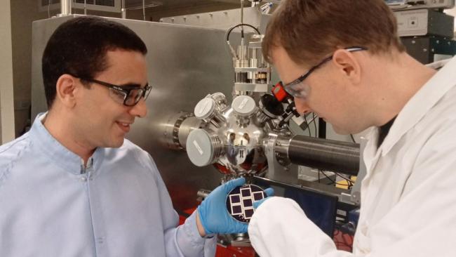
In this project, you will contribute to the development of the next generation of high-efficiency solar cells by developing novel nanolayer materials to address some of the key challenges currently limiting solar cell efficiencies. Specifically, you will employ atomic layer deposition (ALD), an advanced fabrication technique offering atomic-scale control of film thickness and composition, to fabricate novel dielectric and/or transparent conductive materials, including oxides, nitrides and sulphides. You will investigate and optimise their optical and electrical properties using state-of-the-art characterisation techniques, and explore their application as passivating and/or contacting layers in high-efficiency photovoltaic devices including silicon and/or silicon-perovskite tandem solar cells.
You will join a large group of over 25 researchers within the Silicon Solar Cells & Modules group at ANU, and be part of a collaborative team environment, with direct mentorship from supervisors who are leading experts in the field. Photovoltaics research at ANU is at the global cutting edge, spanning the entire spectrum of solar electricity technologies – from solar forecasting, to fabricating high-efficiency photovoltaic cells, to integrating renewables with storage capacity into the grid. Our group is a world leader in silicon photovoltaic device fabrication and characterisation. We develop the next generation of advanced materials and characterisation technology for high efficiency silicon solar cells and modules. New technologies across the entire production chain - covering silicon ingots, wafers, cells and modules - are being developed to address key barriers to further improvements in the performance and cost of silicon photovoltaics. Our partners are the world’s leading experts in silicon materials, device fabrication and characterisation, from both academia and industry, and spanning across the globe. Many of our research outcomes have been successfully commercialised through our industry partners.
The PhD will be undertaken in our state-of-the-art laboratories, making use of our advanced fabrication and characterisation facilities. Our laboratories allow most semiconductor fabrication processes, including diffusion, ion implantation, oxidation, chemical vapour deposition, atomic layer deposition, laser-based cutting and doping, photolithography, wet-chemical processes, metal and semiconductor evaporation, sputter deposition, metal plating, etc. Specifically, in this project you will work extensively with our newly installed materials deposition cluster, including a brand new, state-of-the-art ALD system. Our characterisation facilities include state-of-the-art optical, electrical, and microscopy tools such as luminescence spectroscopy and imaging, spectroscopic ellipsometry, Raman spectroscopy, photoemission yield spectroscopy, Kelvin probe, solar simulators, etc, and you will also have access to other materials characterisation techniques such as Fourier transform infrared spectroscopy, X-ray diffraction, atomic force microscopy, and electron microscopy within ANU. The project will offer an excellent training environment which will equip you to pursue a career in photovoltaics, semiconductors, or general materials research in industry or academia.
Applying
Prospective students graduated or expecting to graduate with degrees in Electrical and Electronic Engineering, Physics, Materials Science, Applied Science, Chemistry, or related disciplines, with a GPA above 8 out of 10, or 3.5 out of 4.0, or high distinction (HD), or equivalent are invited to apply. However, to be competitive for a scholarship, international students will need to have outstanding GPA rankings within their departments (usually the top 5%, preferably top 2%).
If you meet the HDR admission requirements (self-assessment here), please send an email directly to Dr Lachlan Black (lachlan.black@anu.edu.au) with the following information:
- Email subject: Prospective PhD for silicon PV
- Email body: please provide:
- Your background, experience, and research interests.
- GPA / result of each degree.
- If possible, an estimation of your GPA ranking within your cohort. For example: 3rd out of 100, 5th out of 400, top 1%, top 2%, etc.
- Details of any publications, along with DOI links.
- List of any other relevant research achievements.
- When you expect to be able to start your PhD if successful.
- Attachments: CV, academic transcripts, and an additional PDF file which includes certificates of prizes, awards, recognitions or any other supporting evidence.
Initial assessment is based on the information you provide. In case critical information (e.g. GPA results) is missing your application cannot be considered. Obvious mass application e-mails will not be considered. We apologise that due to the large number of applications typically received, it is not possible to respond to all applicants.
We are looking forward to seeing outstanding candidates joining our group. Candidates from diverse backgrounds, including those traditionally underrepresented in the STEM field, are especially encouraged to apply!
Funding Notes
We are offering to support your PhD candidacy for a competitive scholarship application in the field of photovoltaics at the Australian National University (ANU), located in Canberra, Australia. For the successful applicant, the scholarship fully covers the university fees and research expenses, and provides an additional allowance to cover living costs for 3.5 years:
- Living allowance: AUD$ 34,000 per year
- Conference travel allowance: AUD$ 6,000 during PhD
- Relocation allowance: up to AUD$ 2,500
In case your scholarship application is unsuccessful, there may be options to provide alternative funding from upcoming research projects.
References
Relevant overview publications:
https://doi.org/10.1109/JPHOTOV.2018.2797106
https://doi.org/10.1016/j.solmat.2018.07.003
You can find out more about my research interests and previous publications at (https://researchers.anu.edu.au/researchers/black-l) and those of Prof. Macdonald at (https://cecs.anu.edu.au/people/daniel-macdonald).