Surfaces and interfaces are a key site of electrical losses in silicon solar cells, and minimising these losses is essential to realising high-efficiency devices. This involves the development of innovative thin-film materials and stacks that can be applied to silicon surfaces to minimise recombination losses, while simultaneously performing other functions such as allowing extraction of current and minimising parasitic optical losses.
Advanced Passivated Contacts
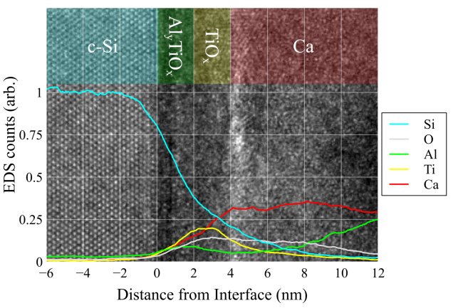
Advanced passivated contact technologies seek to overcome the limitations of existing silicon-based contacts, particularly through improved optical transparency. This area involves significant materials innovation, with a particular focus on transition metal oxides, sulphides, transparent conductive layers, extreme work-function materials, and their combination in contact stacks. At ANU, we investigate innovative new materials and contact structures, fabricated using techniques including atomic layer deposition, plasma-enhanced chemical vapour deposition, evaporation and sputtering, with the goal of obtaining high-performance, optically transparent passivated contacts, suitable for integration in high-efficiency silicon and silicon-tandem solar cells.

Advanced Dielectrics
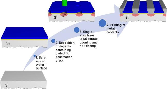
Dielectric passivation materials continue to play a critical role in high-efficiency silicon solar cells due to their excellent passivation properties and unrivalled optical transparency. At ANU we investigate innovative dielectric materials technologies and fabrication processes in order to further drive down surface recombination losses in silicon solar cells. Additionally, we seek to pursue new opportunities for advanced dielectrics to additionally act as dopant or hydrogenation sources, or as gettering layers for bulk impurities. Such multifunctional materials are positioned to simplify device fabrication flows, reducing LCOE and enabling higher-efficiency device architectures.

Interface & Surface Analysis
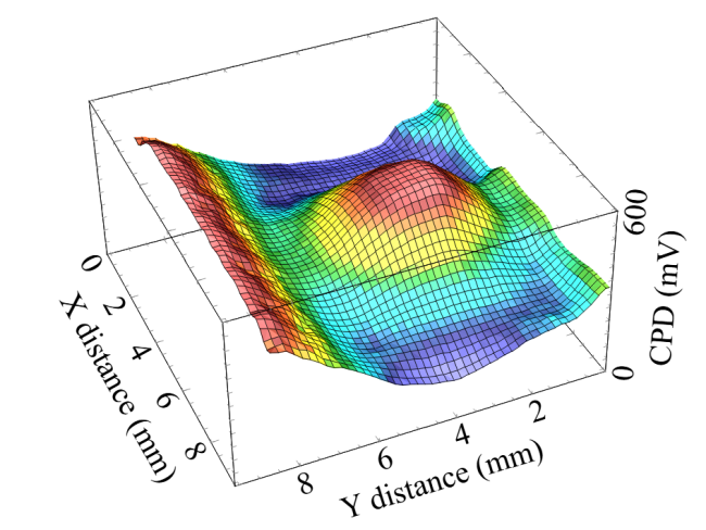
Understanding surface and interface properties is key to engineering passivation and contact structures that can enable high-efficiency solar cells. Within this area we investigate the application of techniques such as capacitance–voltage, impedance spectroscopy, Kelvin probe, and surface photovoltage measurements, to characterise the electronic and energetic properties of surfaces and interfaces in solar cells and correlate these with solar cell performance.
