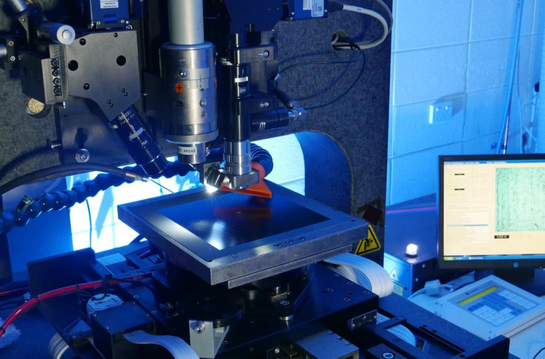
Ultraviolett laser for damage free ablation.
The UV laser with flat top variable spot size is integrated with a high-precision four-axis stage which achieves µm accuracy over a scan area of 200 mm x 200 mm.
Laser ablation
Selective removal of dielectric materials from silicon for opening up regions for local contacts or local doping windows is achieved simply and elegantly by laser ablation. The ideal ablation process is a mimic of photolithography but is by contrast a highly industrially applicable process.
Green, IR or UV lasers can all be used to remove materials with minimal or no damage to the underlying silicon. However, for many of the materials of interest to solar cell manufacturing, UV laser ablation seems the most promising option – offering the ability to remove thin layers of different dielectrics with each laser pulse while resulting in minimal change to surface electronic quality. Dielectric materials currently under investigation include silicon dioxide, silicon nitride, aluminium oxide, and titanium dioxide.
Specifications
- Pulse width: 25 ns
- Wavelength: 248 nm
- Repetition rate: 1-100 Hz
- Pulse Energy: 0 to 4 J/cm2
- Beam profile: Flat top with variable spot size
- Micromachining setup: Four-axis stage with µm accuracy and 200 mm xy-scan range